neuro42-projects
| Home 🏠 Penngineering Projects 🦾 Physics Projects 🔭 Science Communication Projects 🗣 |
Neuro42 Projects 📡
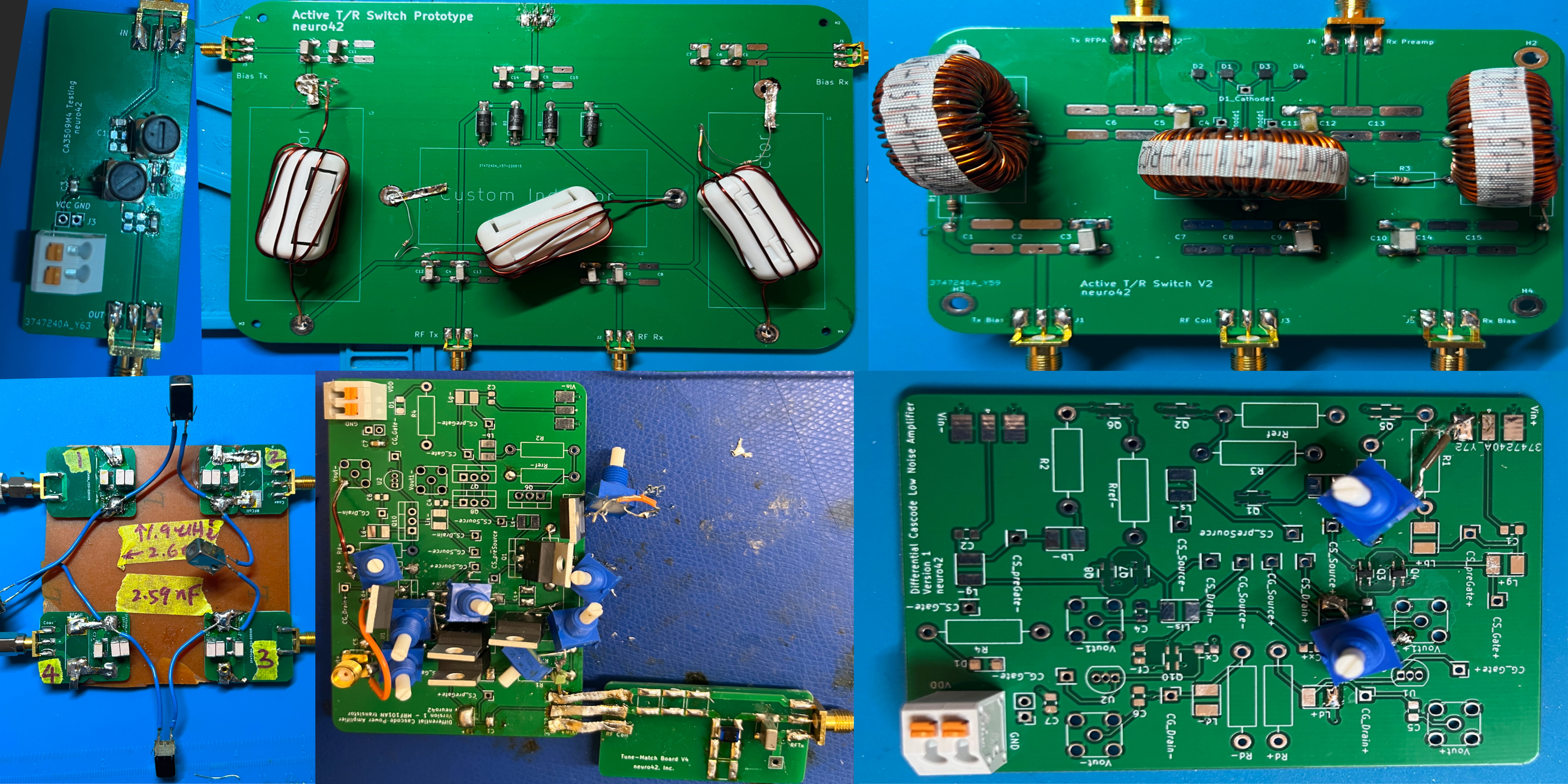
neuro42, Inc. is a medtech Company advancing futuristic technologies for screening, diagnosis, and targeted treatment of neurological conditions. Below is a photo of some of the RF analog circuits I developed during my time there. Further below is information of what I did with them.

Step-Up Voltage Converter
Steps-up a 1.0 V square wave to a 5.0 V square wave.
Researched and simulated different methods of step-up voltage conversion such as non-inverting op-amp, boost converter IC, and non-inverter digital CMOS buffer. Digital CMOS buffer was considered over op-amp due to less SMD resistors requirement and lack of need for additional power supply. Selected digital buffer package, soldered test circuit, and tested its behavior using oscilloscope and function generator.
90 Degree Hybrid
Splits a signal into two with a 90 degree phase and equal (-3 dB) power split
Selected, sourced and soldered appropriate adjustable inductors for the circuit. Successfully tested and tuned its behavior using an oscilloscope and function generator. Designed a PCB for it. Further tested the behavior of other directional couplers in-lab using an oscilloscope and function generator.
Active T/R Switch
Control the direction of current flow during transmit and receive mode, to protect sensitive receive components during high-power transmit mode.
Developed understanding of the circuit schematic working. Designed version 1 of PCB for it. Successfully soldered, tested and debugged its behavior with regular and low power PIN diodes. Designed the final version of PCB for it. Successfully soldered, tested and debugged its behavior with high power PIN diodes. Used oscilloscope and function generator.
Balun & Match
Converts an unbalanced signal (single-ended) to a balanced signal (differential) or vice versa. Designed a PCB for it.
Final Project
Two amplifier versions are required: power amplifier for the transmission line and low noise amplifier for the receive line. These are meant to replace the currently used amplifiers in the transmit and receive line respectively, as they’re expensive. They both are required to produce a gain of around - 18.0 dB and the low noise amplifier is required to have low noise figures of around 0.6 dB. This is difficult as Amplifier ICs for the MRI’s 3 MHz operating frequency are not available on the market due to lack of demand. Most ICs operate at higher frequencies for wirless applications. To circumvent this problem,
- Amplifier ICs whose operating frequencies are higher were investigated
- Amplifiers were designed from scratch
Amplifier IC
Produces a gain of around - 18.0 dB for low noise figures of around 0.6 dB although the signal is distorted
Designed a PCB for it. Used online calculator and network analyser for impedance matching. Soldered, tested, and debugged the circuit using an oscilloscope and function generator.
Differential Cascode Amplifier
Read scholarly articles and textbooks to design schematic for two versions of the differential cascode amplifier: power and low noise. Selected transistors for each. Designed multiple PCBs for it, each for a different transistor or to investigate a different noise reduction technique. Soldered, tested, and debugged multiple amplifier boards along with tune and impedance match boards using oscilloscope, function generator, and network analyser. Successfully built power single-ended cascode amplifier. Differential amplifiers and low noise amplifiers are active areas of research that were unable to be resolved by the end of the internship.